Tutorial: Laying out your first printed circuit board with CPCB
In this tutorial we will lay out the DC version of the opamp circuit we designed previously. I am going to assume you have saved that circuit as “dc-amp.cschem” somewhere on your computer. If you don’t have it handy, you can download a copy here.
First step: Starting CPCB
If you have used the CSchem installation package on Windows, or the :file:.deb package on Linux, you should be able to find CPCB in your computer’s start menu.
Alternatively, you can start CPCB by typing
cpcb
into a terminal.
Either way, you will be presented with an empty layout:
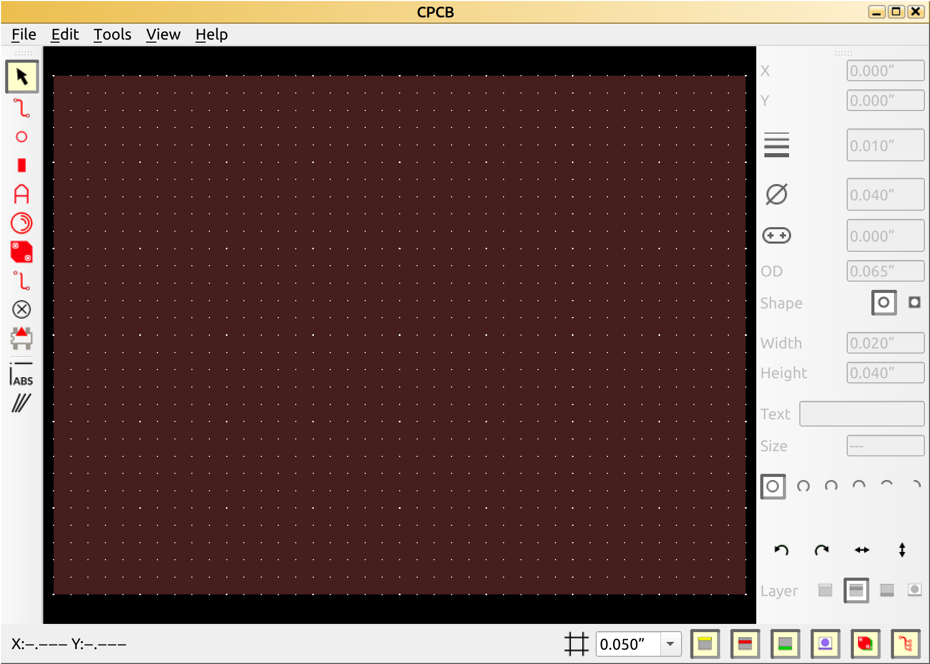
You will immediately notice that the CPCB user interface is not quite as sparse and elegant as that of CSchem. The reason is that in drawing PCB layouts, you have to interact with physical reality, which means there are many more knobs to turn. However, you will hopefully soon agree that CPCB is pretty easy to use. The main components of the user interface are:
The actual layout in the center;
A button bar on the left to select editing mode;
A “properties” bar on the right to set parameters on components and traces;
A status bar on the bottom where you may hide and show various things, and define a snapping grid.
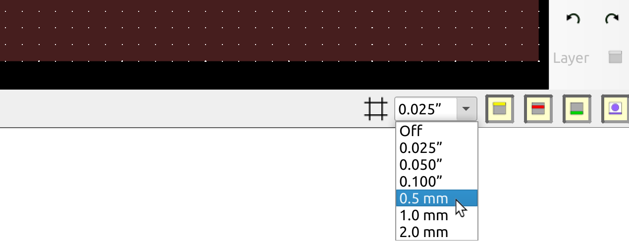
As you may notice, the default system of units in CPCB is inches. This is because many through-hole components are defined on a 0.1 inch grid. That said, CPCB is equally happy with metric units: Just press the little arrow next to the grid selector, and select a metric grid spacing.
Parts, components, outlines, footprints: it’s all the same
In laying out printed circuit boards, the parts placed on the board are commonly called “component outlines”, or just “outlines” for short. Some other software uses the term “footprint”. It’s all the same from our perspective.
There are so many electronic parts in the world, that it seemed futile to provide a small library of common ones in a side panel. Therefore, CPCB comes with a more extended library stored in a folder hierarchy on your computer. Start by opening this library: Choose “Open library” from the “Tools” menu, then navigate to System → Through-hole → Connectors.
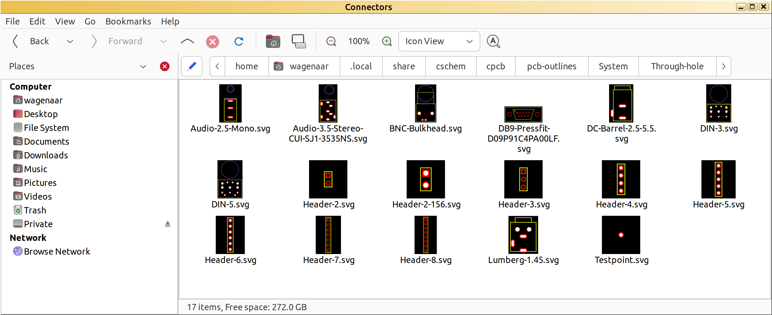
CPCB stores its component outlines as svg files with key information stored in meta tags. The only reason you need to know this, is that it means that your operating system should be able to display thumbnails for CPCB outlines. If it doesn’t, it is worth seeing if you can a better file manager.
Linking schematics and PCB layouts
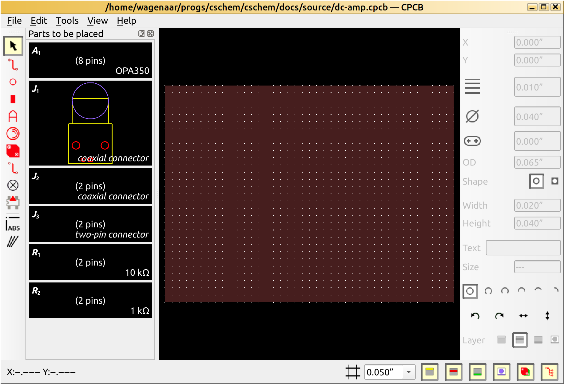
We could at this point start to simply drag components onto the board from the file manager, but to make our lives a little easier, let’s first inform CPCB that we are implementing our opamp schematic. Choose “Link schematic” from the “Tools” menu, and navigate to our previously created “.cschem” file. If you now choose “Show parts to be placed” from the “View” menu, CPCB can guide us in the placement process:
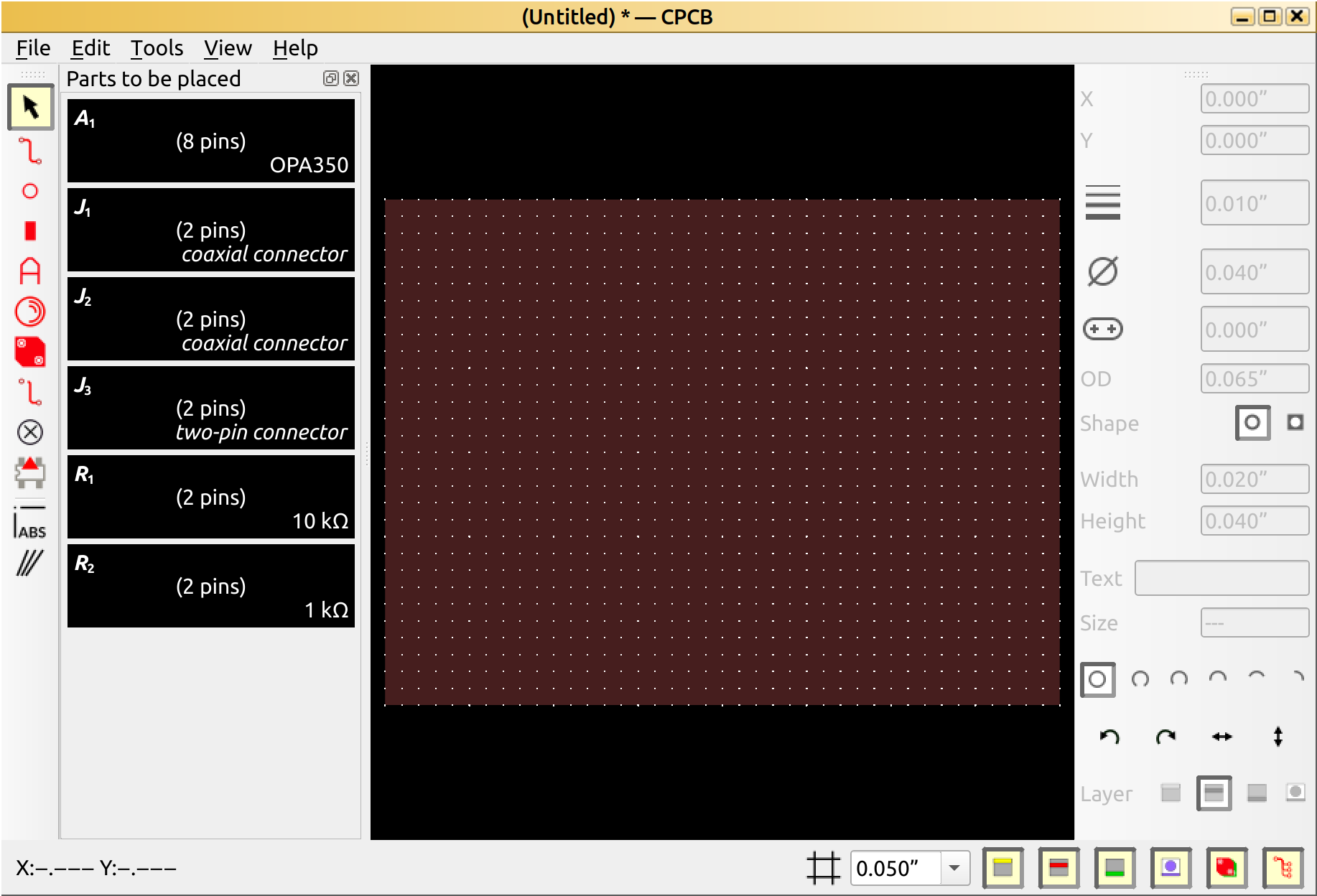
Based on the information in the schematic, CPCB has figured out that A1 is an 8-pin device, and even though we never assigned a part number to the various connectors, from the symbol we chose, it inferred we intended to use coaxial connectors for J1 and J2. (Don’t worry if you had different plans, you are free to ignore CPCB’s inferences.)
Selecting components
We could just drag the various components straight onto the PCB from the file manager, but a more convenient workflow is to drag them into the “Parts to be placed” panel first. That way, we get a better sense of how large various things are.
Begin by dragging the “BNC bulkhead” connector from the “Connectors” folder onto J1.
Then, drag it from there onto J2. Now drag the DC-Barrel-2.5-5.5 connector onto J3. Navigate to the “Passives” folder and drag the “Resistor-¼W” over to R1 and R2. Finally, navigate to the “Sockets” folder and drag the “dip-8” socket over to A1.
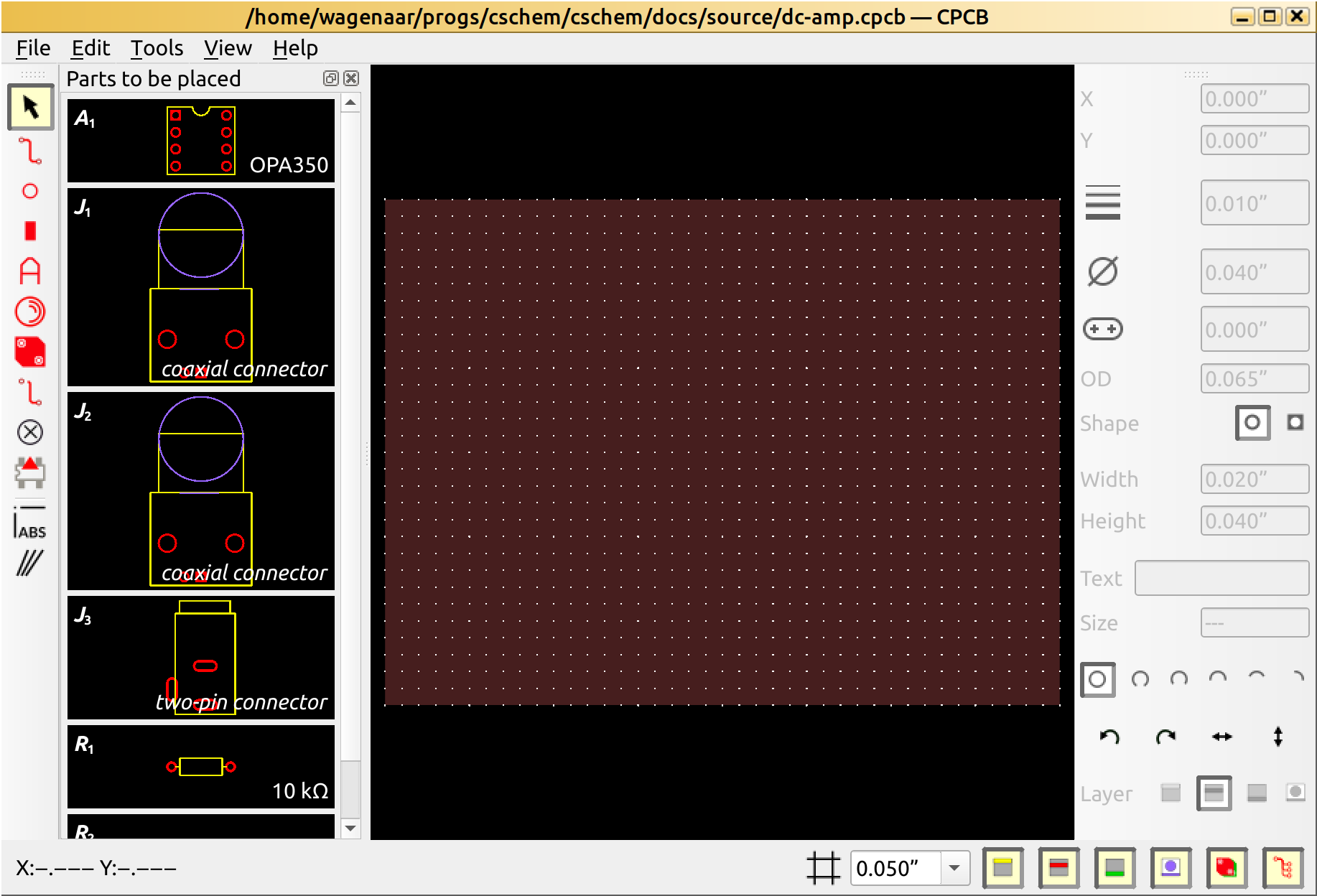
That gives a pretty good sense of how much space we are going to need.
Placing components
Let’s start our layout by placing the connectors along the top edge of the board, and the amplifier IC below the two BNC connectors. Drag each component from the “Parts to be placed” panel onto the board in turn. Notice that the parts snap to the grid, and that parts disappear from the side panel once placed.
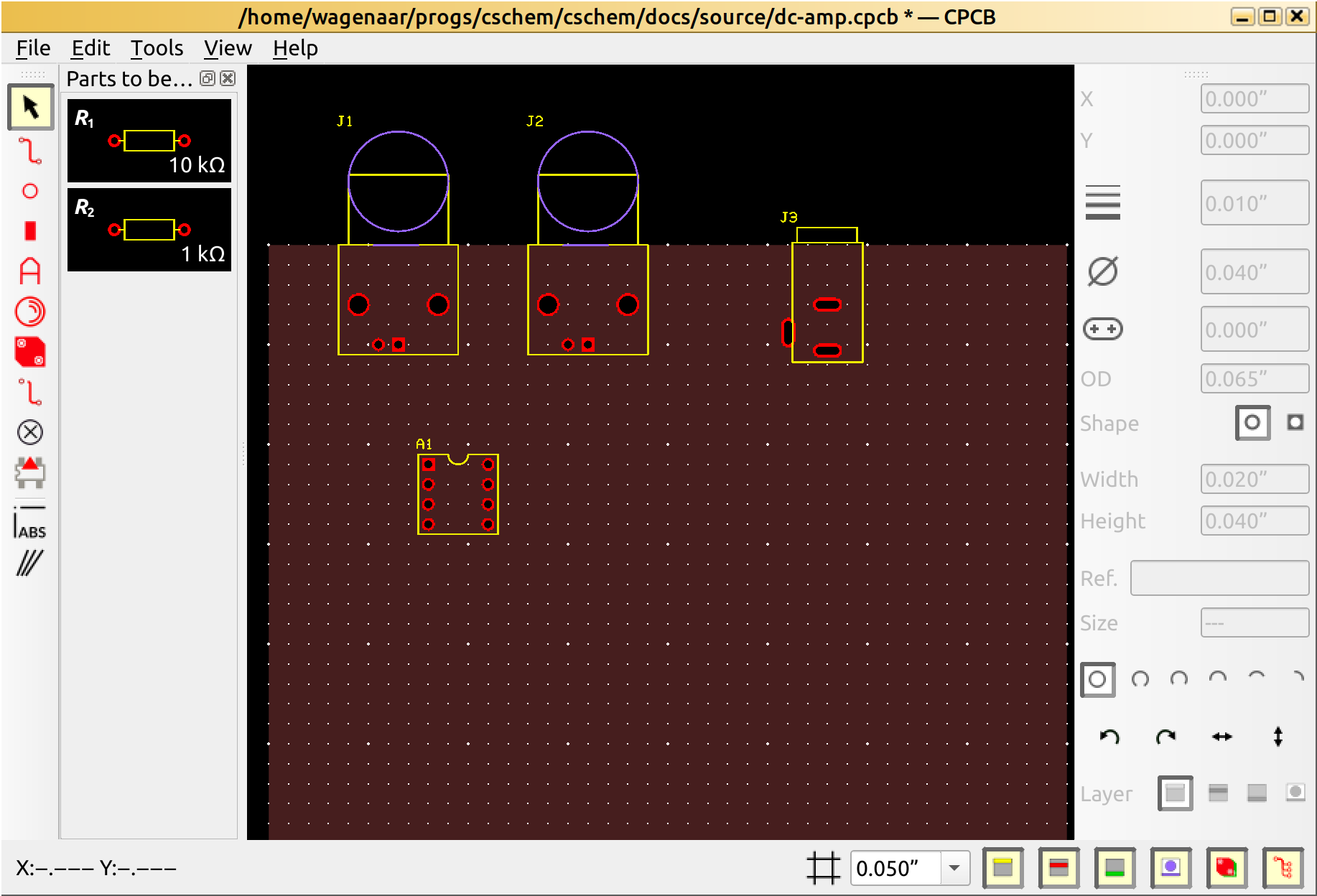
CPCB naively placed the part identifiers (a.k.a. “references”) in the air for all three connectors, but we can easily drag the texts onto the board. Let’s also place the two resistors near A1.
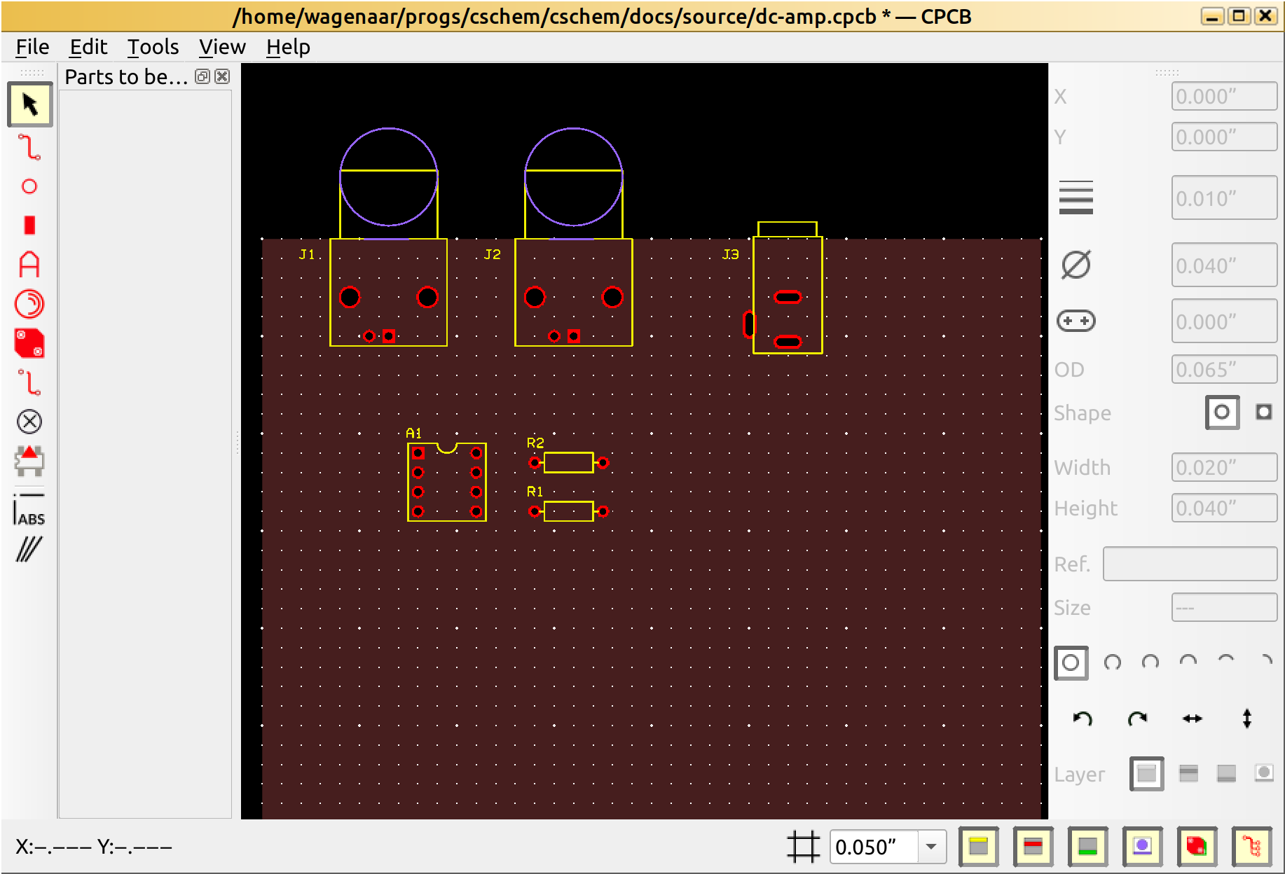
This layout is likely to be reasonable, but we might fine-tune it once we have some connections made.
Laying out a ground plane
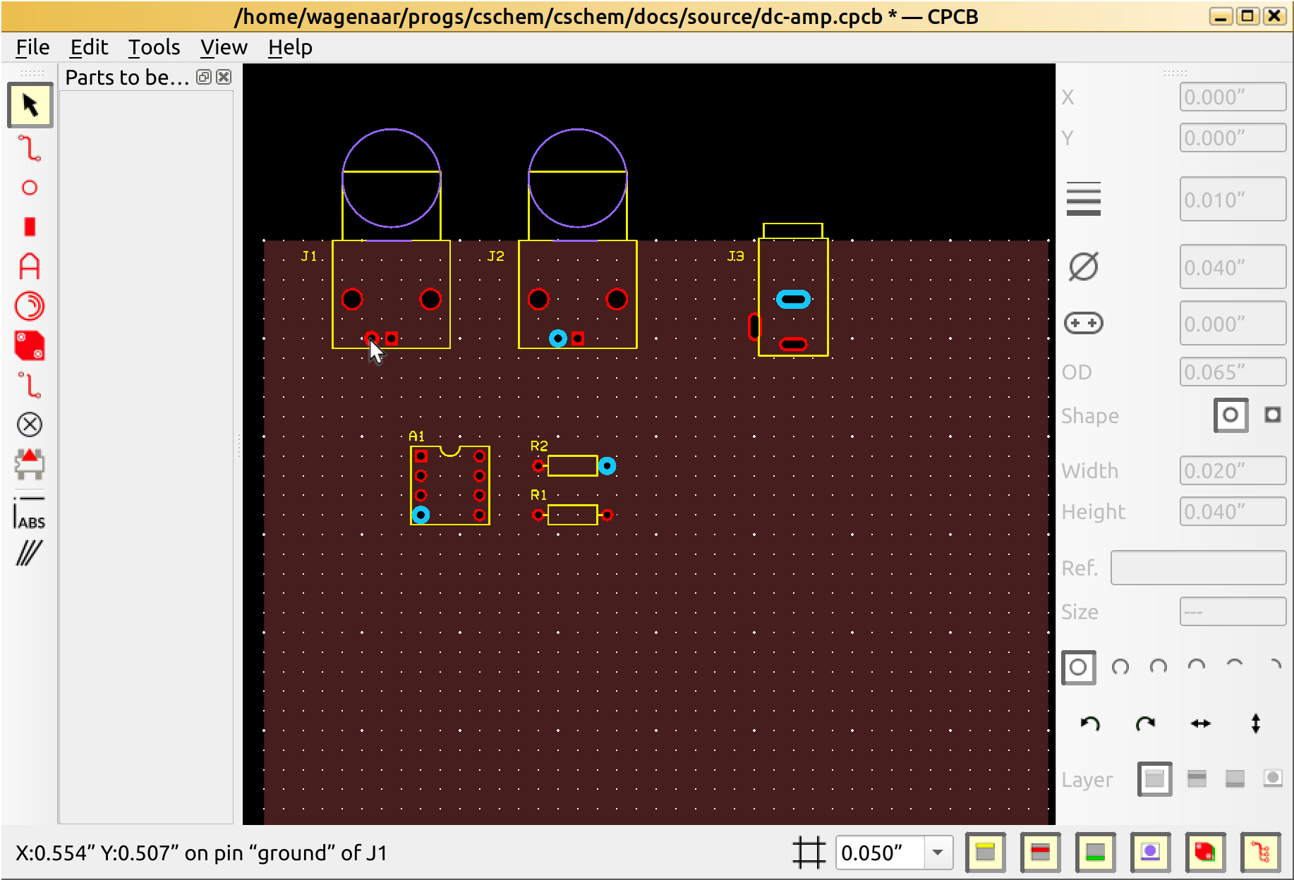
If you move the mouse around the layout and hover over various pins, CPCB will tell you were that pin should connect to. For instance, if I hover over the ground pin of J1, it tells me there are lots of other pins that need to be connected to ground:
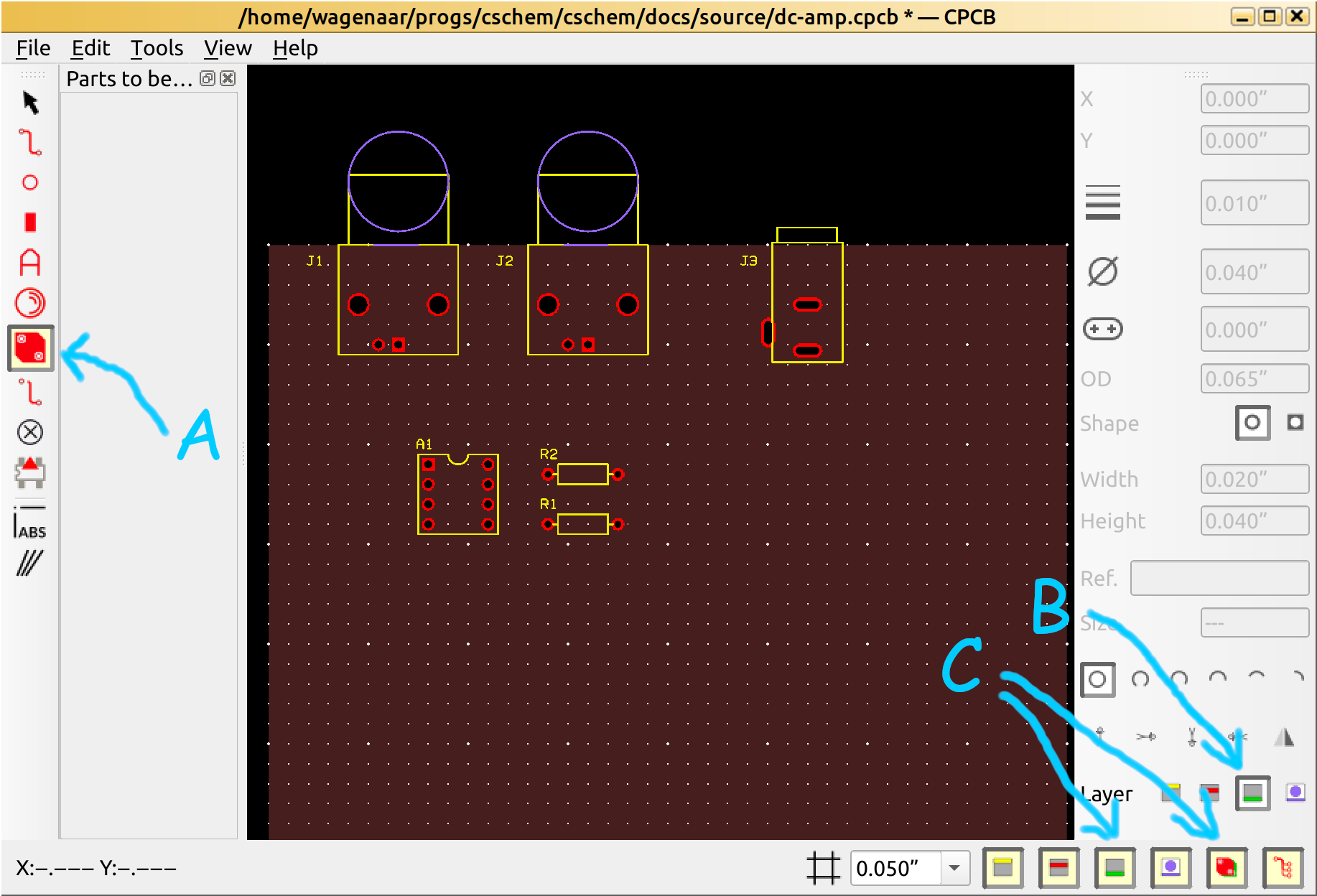
Rather than drawing all of those as individual traces, it is convenient to create a “filled plane” to replace all the ground connections. To do so, press “F7” or select the “Filled planes” icon in the button bar on the left of the screen (marked “A” in the image below). Next, press “3” or click the “bottom” layer button in the properties area on the right (marked “B”). We are going to place our ground plane on the bottom side of the PCB. So, lastly, make sure that both the bottom layer and the filled planes are visible (using the buttons marked “C”).
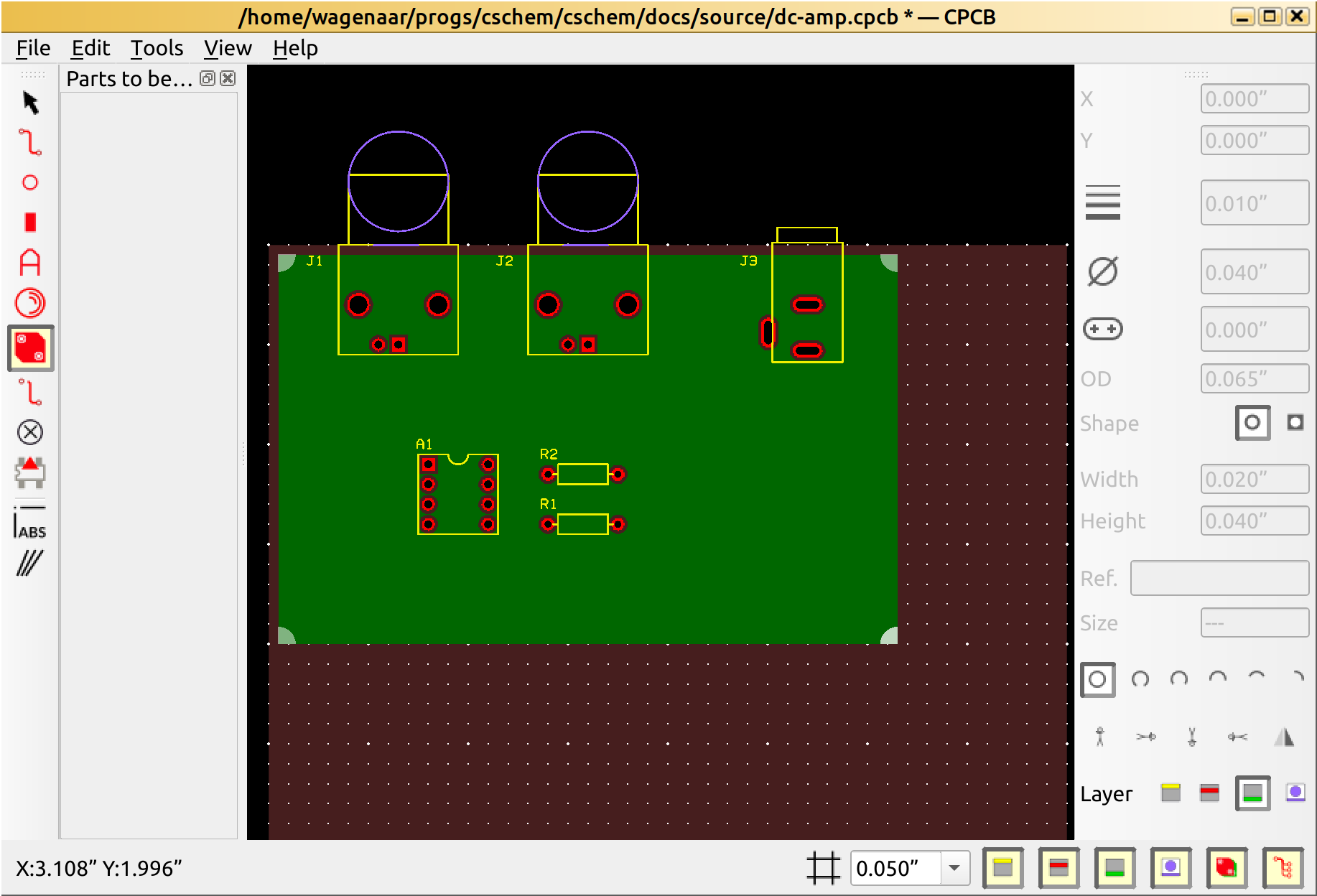
To actually create the filled plane, simply drag a rectangle out over the area of the board you want to fill:
(You can change the shape later by dragging the corners or an edge. You can also create additional vertices by holding Shift while hovering over an edge.)
Once the plane is created, it is convenient to hide it. So press Ctrl+F5, or click the button in the bottom right of the screen.
Making connections
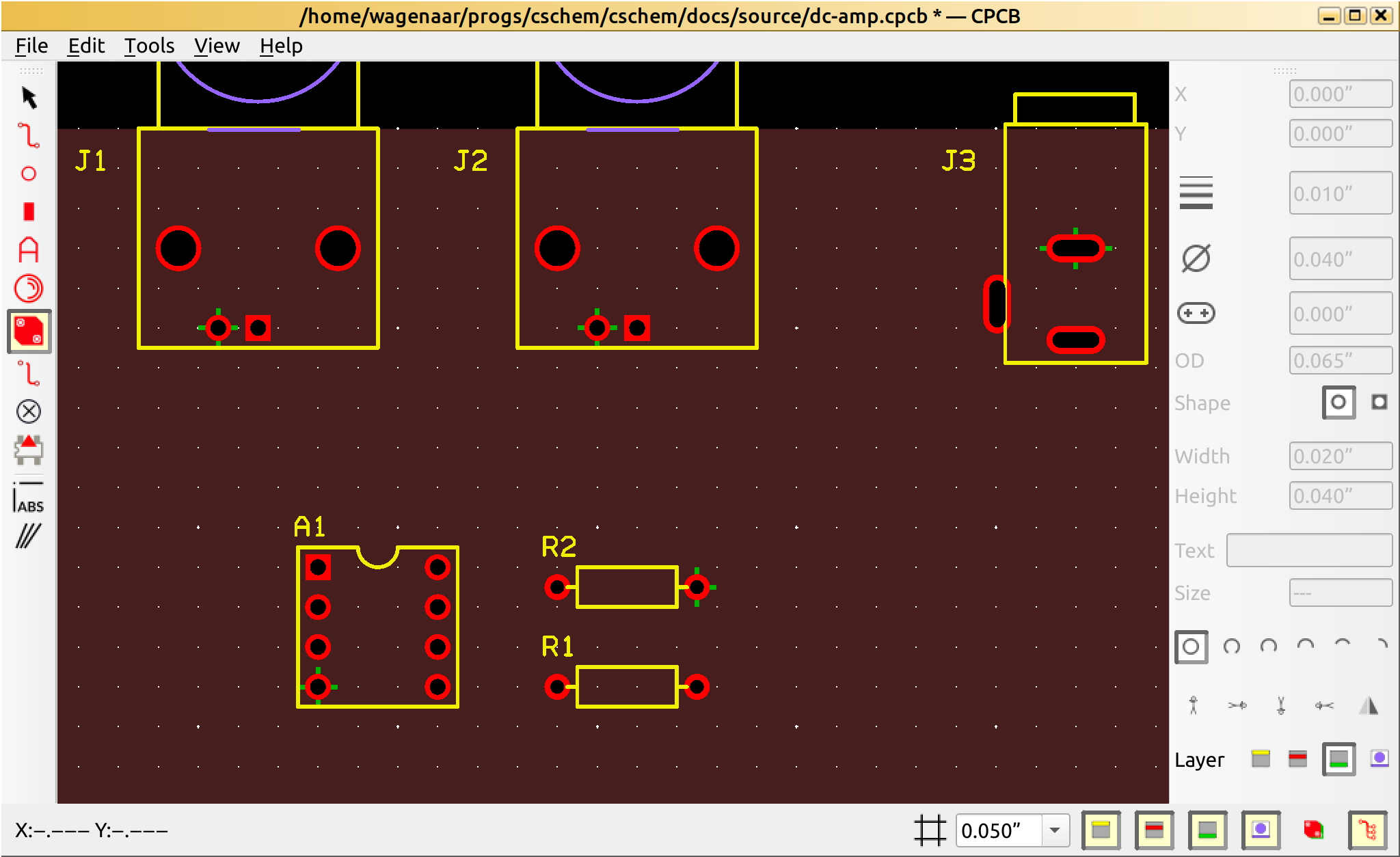
When making connections, I like to zoom in a little. Still with the bottom layer selected (press “3” just to make sure), double-click the ground pin of J1. A small green cross appears, indicating a connection to the filled plane. As you hover over this pin, all the other pins that need to be connected to ground light up blue. Double-click them one by one.
Wasn’t that fast progress? Now let’s make the rest of the connections. For a simple board like this, we can probably get away with laying most of them on the top layer, so let’s start that way. Press “2” to select the top layer, and “F2” to select the tracing tool. Hover over any unconnected pin and watch the blue highlights pop up. I like to make short-range connections first, so I am going to work on the connections between the resistors and the opamp. Hovering around, it strikes me that the connections would be easier if the resistors were rotated, so go back to “Edit” mode (F1), drag a selection rectangle over the resistors, and rotate them counter-clockwise, along with their texts (Ctrl+Alt+Shift+R, or use the “Edit” menu). Now, press “F2” again, and click on a pin to start dragging out a connection. If the line looks yellow, you’re not drawing on the intended layer, so press Escape to abandon the operation, then “2” to make sure you are drawing on the top layer, and try again. It is OK to draw straight through yellow lines with your red trace.
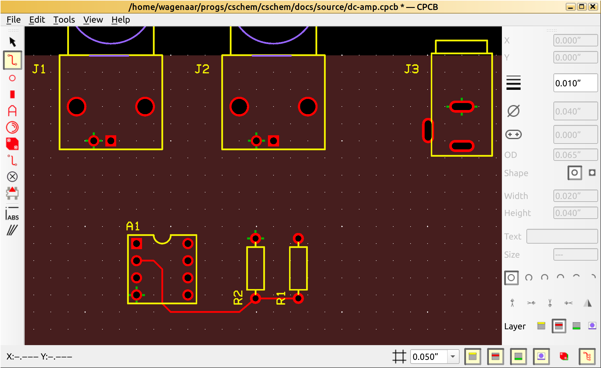
Make as many elbows as you need to lay out a clean trace. I like to stick to horizontals and verticals with short 45-degree connector bits. If you press “F12”, CPCB will even enforce that constraint.
Hover around other unconnected pins to see what remains to be done. Working from short-range to long-range tends to be easiest.
When you think you’re done, choose “Verify nets” from the “Tools” menu, to see if CPCB agrees you made all necessary connections.
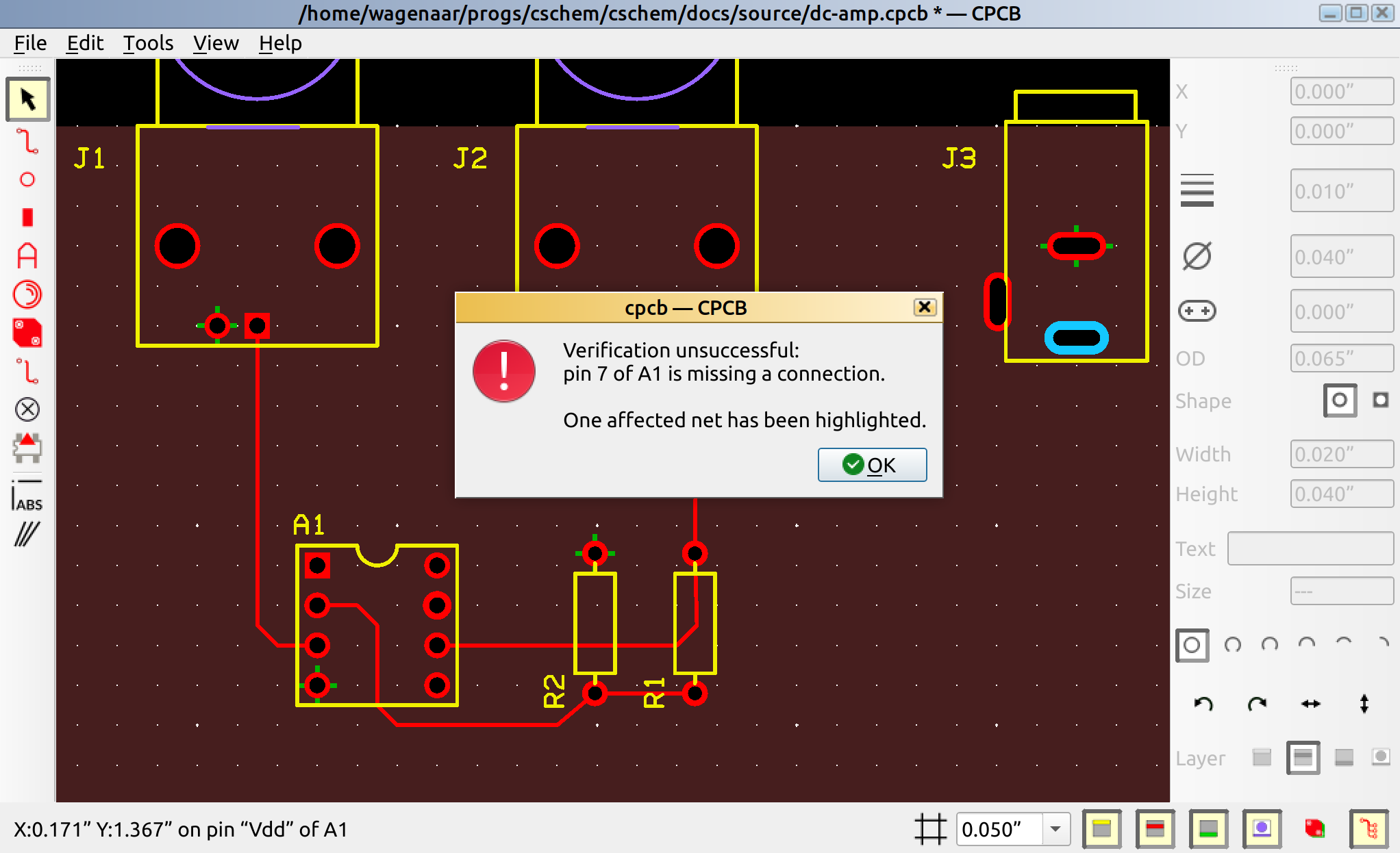
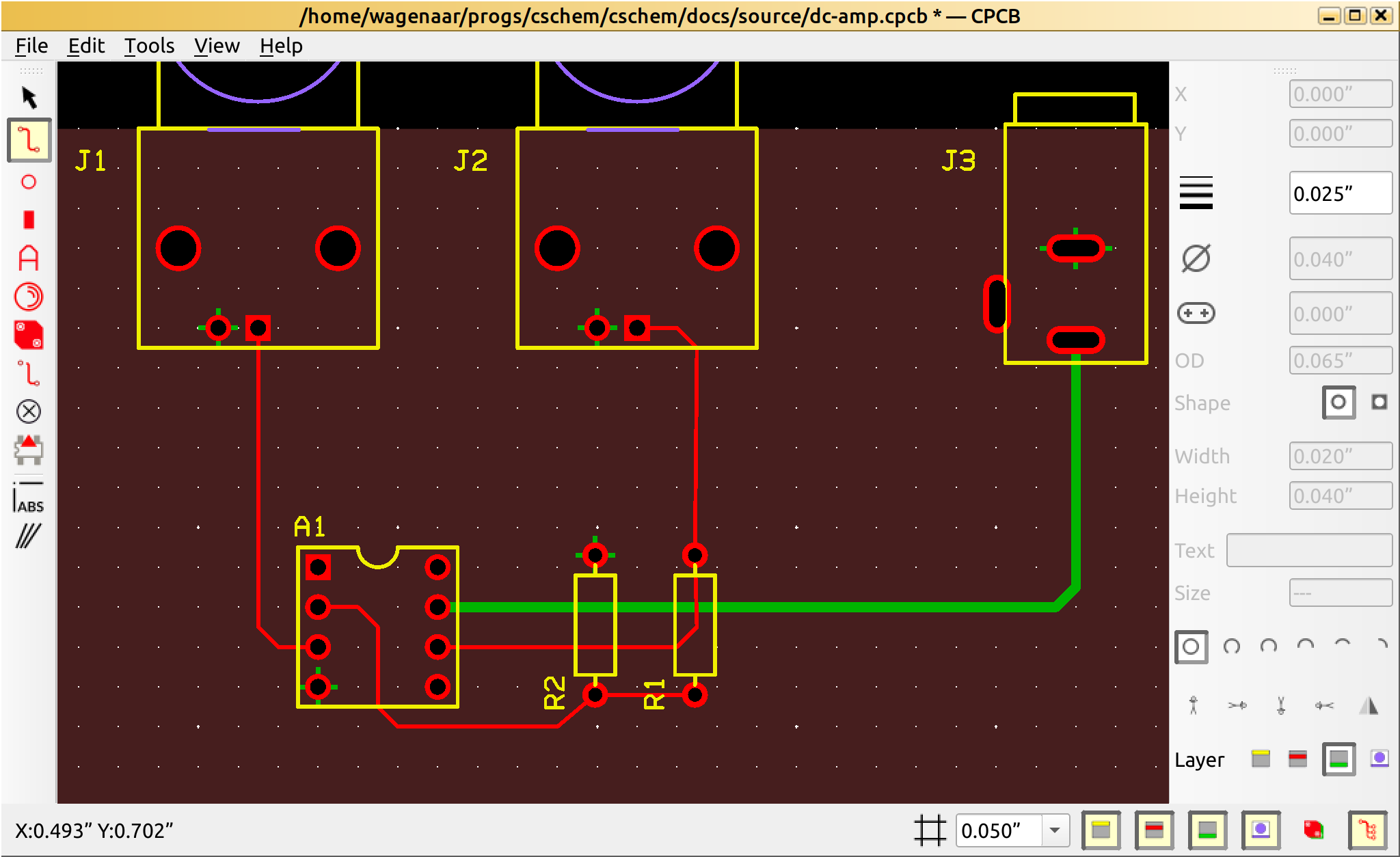
Ah yes! We still need to connect 5V to the opamp. Let’s make a nice thick trace on the bottom layer for that. Press “3” to select the bottom layer, then type “0.025” into the linewidth box. (It’s the only box that’s not grayed out on the right while in “Trace” mode.) Now hover over the pin that was shown in blue, figure out where it needs to be connected, and make the connection.
All done? Let’s do another round of “Verify nets”. CPCB should respond “All nets verified OK.”
Tidying up
Let’s spend a few minutes tidying up the design by pulling things a little closer together. I also like to have mounting holes in my PCBs, so I press “F3” for “Hole” mode (or click the button [1]), and set the diameter to 0.125 inch (good for US #4-40 screws or M3 alike).
Let’s place some identifying text on the board as well, by pressing “F5” (or clicking the button), then clicking on the board in the desired location of the text. (The text can of course be moved later if you don’t get it quite right the first time.)
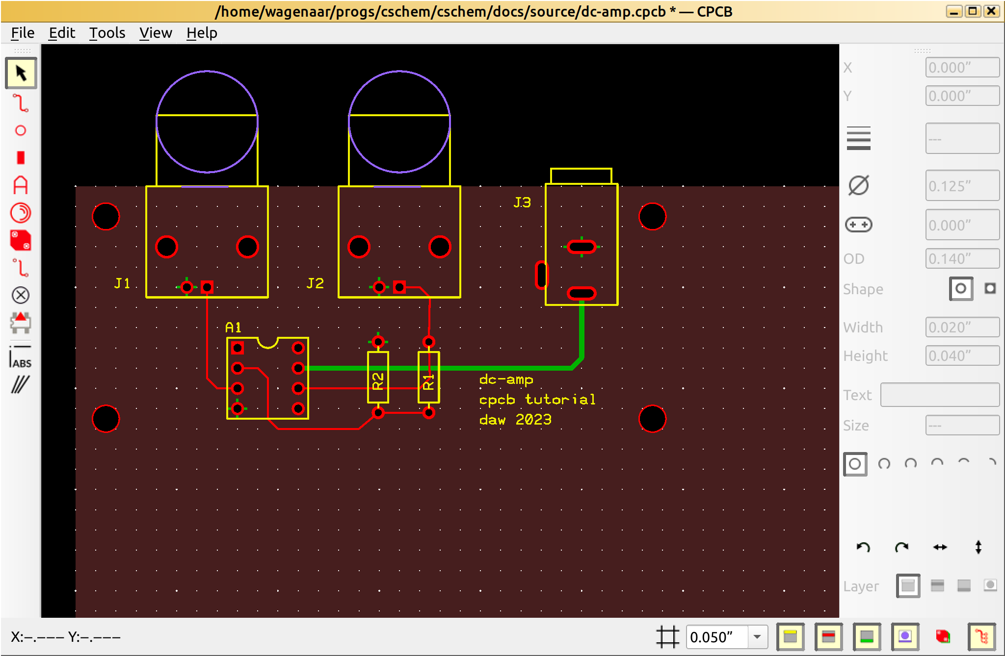
The board is a lot bigger than it needs to be, but before we can shrink it, we first have to adjust the filled plane so it doesn’t stick out too far. Press “Ctrl-7” (or click the button) to unhide the filled plane, then press “F7” (or click the button) to enable editing it. Drag the right and bottom edges to a reasonable position.
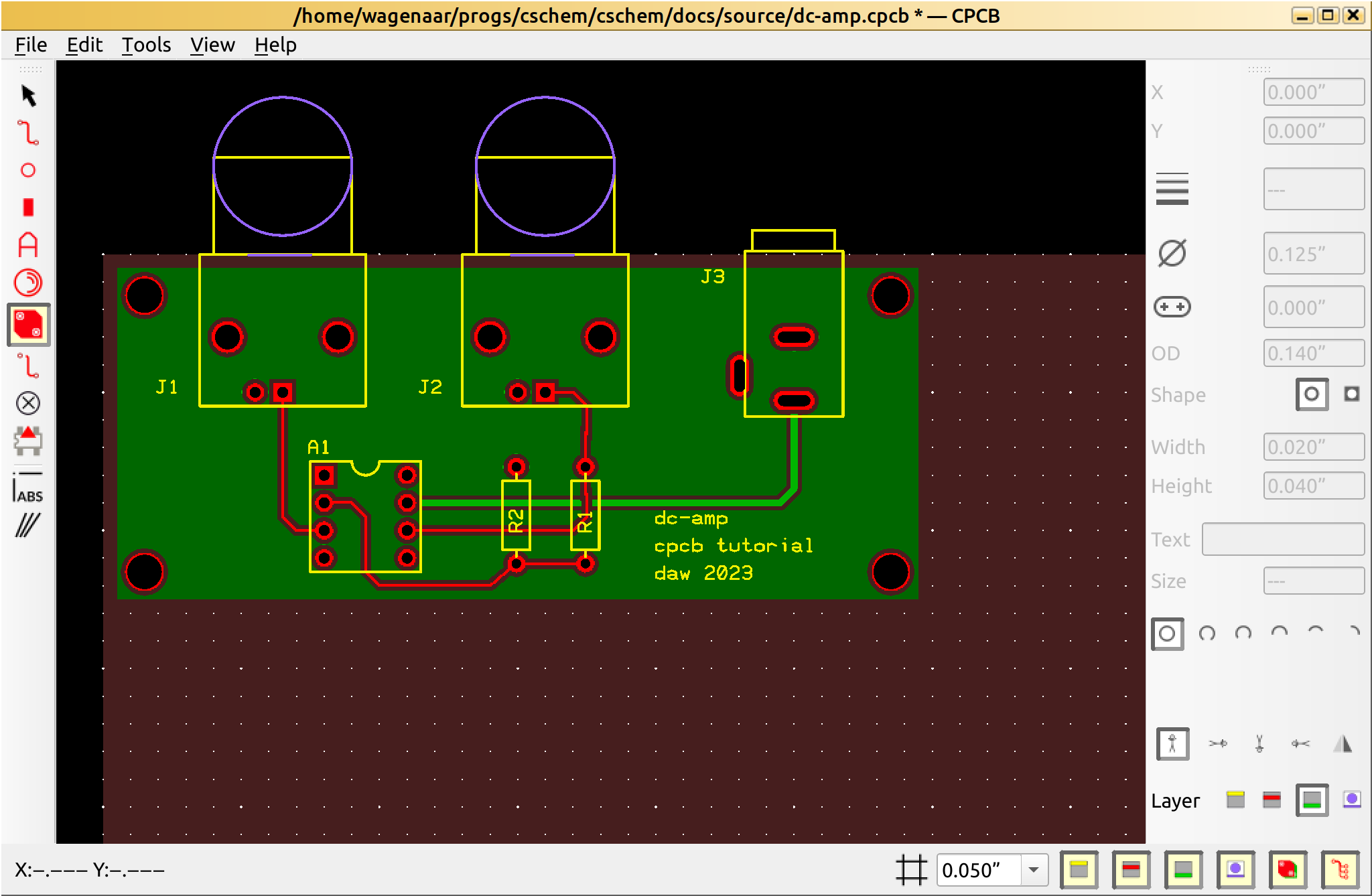
Notice, by the way, how the filled plane automatically avoids the power trace we drew a minute ago?
Finally, choose “Board size” from the “Tools” menu, click “Shrink”, then “OK”.
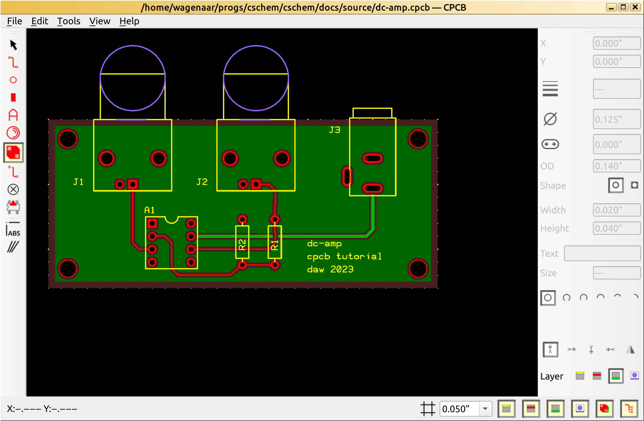
Now, we should be all done. Let’s do one more “Verify nets” to be positive.
Good?
Getting your board manufactured
One might reasonably choose to lay out the board we just drew on a breadboard by hand, but for slightly more complex designs, having a custom PCB manufactured is a great convenience. Once you are sure your design is good, choose “Export fabrication files” from the “File” menu.
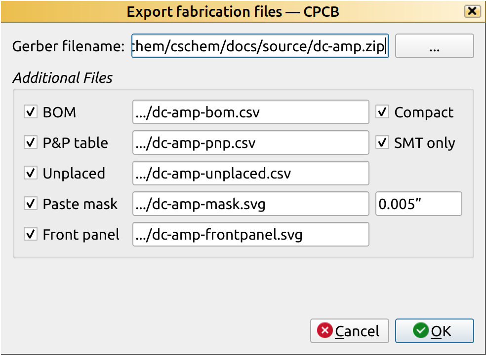
This creates a lot of files. The only one we need right now is the “Gerber” file, which is actually a zip archive containing instructions for board manufacturers. The other files that are generated are:
BOM (“Bill of materials”): a shopping list for your parts;
P&P table: instructions for a “pick and place” service that may do the soldering for you;
Unplaced: a list of any items that CPCB could not include in the P&P table;
Paste mask: a design for a stencil you can use for placement of surface-mount components;
Front panel: a design for a front panel, if you are going to put the final product in an enclosure.
Usage instructions for all of these can be found in the user guide. If you don’t want to clutter up your project folder, just unselect all of the options.
Click “OK” and send the zip file to your favorite manufacturer. (There are lots of companies that do excellent work. Unless you use extremely thin traces, they are probably all plenty good enough, so you can afford to select based on other criteria, such as geographical proximity. The one thing to always check is that they will use lead-free processes for your manufacture. Shockingly, that is still not a given in this industry.)
Footnotes